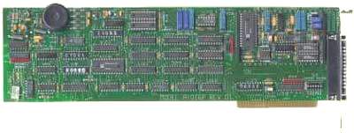
AD12-16/16F
ISA Bus Analog and Digital I/O Card
Features
- 16 Single-ended or eight differential inputs
- 12-bit resolution with five input ranges
- Additional gain setting set by resistor
- 50,000 samples/second (AD12-16)
- 100,000 samples/second with DMA(AD12-16F)
- On-board pacer clock and counter/timers
- Two multiplying 12-bit D/A converters
- Eight digital I/O lines (4-in and 4-out)
- Programmable scan rate
- Supports DMA and interrupts
- Designed, made, supported, and manufactured in the USA
ANALOG INPUTS
The cards accept up to eight differential or 16 single-ended analog input channels. Inputs are protected against over-voltages up to ±35V and, typically, can survive static discharge beyond 4000V. When power is off, the inputs are open-circuited providing fail-safe operation and continue to offer overvoltage protection up to ±20V. The channel input configuration is switch selectable on the card providing a choice between 16 single-ended channels or eight differential channels. In the latter case, common mode rejection ratio is a minimum 86 db and common mode voltage range is ±11V.For applications where negligible time skew between channel samples is desired, AD12-16 or AD12-16F can be used in conjunction with one or two SSH-08 Simultaneous Sample and Hold cards. Further, if aliasing of analog input signals is a consideration, then AD12-16 or AD12-16F can be used with one or two AAF-xx Anti-Alias Filter cards. In this case, specify AD12-16-S02 or AD12-16F-S02.
Inputs are amplified by a low-bias-current, fast-settle-time, high-common-mode rejection, monolithic instrumentation amplifier with switch selectable gains of 0.5, 1, 2, 5, and 10. Use of those gains provides voltage ranges of 10, 5, 2, and 1 volts unipolar and ±10, ±5, ±2.5, ±1, and ±0.5 volts bipolar. The amplifier has exceptionally low input leakage current; 125 picoamps typical at 25°C. Competitor designs are rated at 250 nanoamps typical! Also, the amplifier settles to 0.01% in 4 µSec and CMRR is 90 db at 10 KHz.
In addition, you can set up a special range by installing a single gain-setting resistor. Gain selection is via switches which are accessible from outside the computer through a cutout in the mounting bracket. Thus, if a card is already installed, the range can be changed without dismounting the card.
AD12-16 uses an industry standard, 12-bit successive-approximation analog-to-digital converter (A/D) with a sample and hold amplifier input. Under ideal conditions, throughputs of up to 50,000 conversions per second are possible. (AD12-16F uses a faster A/D and throughputs up to 100,000 conversions per second are possible.) A/D conversions may be initiated in any one of three ways: (a) by software command, (b) by on-board programmable timer, or (c) by direct external trigger. In turn, data may be transferred to the computer by any of three software selectable methods: (a) by program transfer, (b) by interrupt, or (c) by direct memory access (DMA).
INPUT SYSTEM EXPANSION
The card can be used with up to sixteen external AIM-16P analog-input expansion cards. (This necessitates converting some digital inputs to digital outputs as will be described later.) Each AIM-16P card provides capability to 16 differential inputs and thus, there can be up to a maximum of 256 inputs per combination of AIM-16P's and AD12-16 (or AD12-16F). The first AIM-16P is connected to the AD12-16/16F by a CA37 cable adaptor and a flat ribbon cable and any additional AIM-16P cards are daisy-chained to each other by ribbon cables.DISCRETE DIGITAL I/O
Four bits of TTL/CMOS-compatible digital input capability are provided. Digital inputs IP0 and IP2 have dual uses. Input IP0 provides an external trigger for the A/D or for Counter/Timers 1 and 2. Input IP2 provides an input to enable Counter/Timer 0. These inputs can be converted to output ports for multiple AIM-16 applicat ions as described under Input System Expansion. When this is done, you give up capability for external triggering the A/D and gating Counter/Timer 0. Four bits of digital output are available with LSTTL logic levels and 10 LSTTL load drive capability. Discrete outputs OP0 through OP3 provide multiplexer addressing capability for input expansion card use, as described previously, or as separate digital outputs.COUNTER/TIMER
The card contains a type 8254 Counter/Timer which has three 16-bit programmable counters. Counter/ Timer 0 is enabled by a digital input and uses either an internal 100 KHz clock or an external clock of up to 10 MHz as selected by user software. This Counter/Timer is not committed on the card. It's clock, enable, and output lines are available to you at the I/O connector. Counter/Timers 1 and 2 are concatenated and form a 32-bit Counter/Timer for timed A/D trigger pulses and/or for external frequency generation. The dual Counter/ Timer can be enabled by program control and clocked by a jumper-selected 1 MHz or 10 MHz on-board crystal oscillator source.Counter/Timer 0 and Counter/Timers 1 and 2 can be set up for event counting, frequency or period measurements, and pulse or waveform generation. Also, Counter/Timers 1 and 2 can be jumper programmed to initiate A/D conversions.
ANALOG OUTPUT
The card has two multiplying 12-bit digital-to-analog converters (D/A) connected to output drivers capable of providing 5 mA current drive. Each channel provides an output of 0 to +5 VDC if the internal -5V reference voltage is used. That on-board reference voltage can be replaced by an external ly supplied reference voltage (biased AC or DC) by jumper selection. In this case, the D/A's will operate as multiplying D/A's with two quadrant capability. The maximum external reference voltage that can be applied is -10 volts.If the analog outputs are to be used for control, please specify AD12-16-S01 rather than AD12-16. That variant includes a modification that forces the D/A converter outputs to zero at power-up (or whenever there is a hardware reset). This assures that there will be no accidental output until a computer write enables these outputs. There is no extra charge for this modification.
If analog outputs are not needed in your application, specify Model AD12-16-S03 which is lower cost.
INTERRUPTS AND DMA
Interrupts can be initiated by completion of an A/D conversion or by DMA terminal count if programmed by software. Interrupt levels 2 through 7 are available. Software control of direct memory access for transfer of A/D conversion data to the computer is supported at either level 1 or level 3 as switch selected.TRANSFERRING DATA INTO THE COMPUTER
The cards have been designed using state-of-the-art components to provide high data throughput using the DMA capabilities of the computer. Direct memory access is the most satisfactory way to transfer data from the A/D to memory at rates over 10,000 samples/second because, at this speed, program transfers through the CPU become difficult to handle in the short time available between conversions.Also, program transfers are subject to disruption by other interrupt processes in the computer. Use of real-time triggering of the A/D plus DMA assures synchronism in sampling that is unaffected by other computer operations. That capability is essential in applications such as signal analysis, fast Fourier transform, and vibration and transient analysis where high data rates must be sustained for short intervals of time.
Thus, AD12-16/16F's open I/O mapped architecture together with three modes of data transfer (programmed via CPU, interrupt via CPU, and DMA) provides considerable application flexibility.
REFERENCE VOLTAGE AND POWER REQUIRED
A -5.0V (±0.05) reference voltage is available from the A/D reference source for external use. This reference output can source up to 5 mA of current. The card requires only +5 VDC and +12 VDC from the computer power supply. An on-board DC-DC converter translates the 12 VDC to low noise, isolated ±15 VDC for the precision analog circuitry.Downloads
Available Reference Manuals
- View / Download the AD12-16F Manual (.PDF)
- View / Download the Software Reference Manual (.PDF)
Available Software Downloads
Drivers and Downloads
Full list of available Downloads: Software Packages, Drivers, Manuals, and other documents
Custom Software
ACCES also offers Custom Software Services for our products. Our prices are unbelievably low, often as inexpensive as free! If you need something tweaked to support your needs, or an entire enterprise application developed from scratch, it is definitely worth your time to inquire with us, first.
Further information about available ACCES Software:
- Redistributing Windows Drivers
- A list of ACCES drivers and the files that compose them under different versions of Windows, so you can easily redistribute ACCES cards and drivers.

Analog Inputs
- Channels: Switch selectable, 8 differential (Hi/Lo/Gnd) or 16 single-ended.
- Resolution: 12 binary bits.
- Accuracy: Can be calibrated to 0.01% of reading ±1 bit. At Gain 1, 2, 5, 10: 0.002% typical, 0.04% max. w/o recalibration.
- Input Voltage Range: Switch selectable, ±10V, ±5V, ±2.5V, ±1V, ±0.5V, or 0-10V, 0-5V, 0-2V, 0-1V.
- Coding: True binary for unipolar inputs and offset binary for bipolar inputs.
- Overvoltage: Continuous single channel, to ±35V without damage.
- Input Current: 1.1 nA maximum, 125 pA typical at 25°C.
- Temp. Coefficient:Gain: ±50 PPM/°C at gain 0.5, 1, and 10, 78 PPM/°C at gain 2, and 63 PPM/°C at gain 5.
Zero: ±27 PPM/°C maximum at gain 10, ±107 PPM/°C maximum at gain 1.A/D Specification
- Type: Successive approximation.
- Resolution: 12 binary bits.
- Conversion Time: AD12-16: 15 uSec max., 12 µSec typical.
AD12-16F: 9.5 µSec max., 7.5 µSec typical.- Monotonicity: Guaranteed over operating temperature range.
- Linearity: ±1 bit.
- Zero Drift: ±10 PPM/°C maximum.
- Gain Drift: ±45 PPM/°C maximum.
- Trigger Source: Software selectable, external trigger, programmable timer, or program command.
Sample and Hold Amplifier
- Acquisition Time: 1 µSec to 0.01% typical for full scale step input.
- Aperture Uncertainty: 0.3 nSec typical.
- Reference Voltage Output: -5.0 VDC ±0.05 VDC.
- Temperature Coefficient: ±30 PPM/°C.
- Load Drive: ±5 mA maximum.
D/A Specification
- Channels: 2, independent.
- Type: 12-bit, double-buffered, multiplying.
- Linearity: ±1/2 bit.
- Monotonicity: ±1/2 bit.
- Output Ranges: 0 to +5 VDC when using the -5V reference. May also be used with other DC or AC reference input. Maximum output limit ±10V.
- Output Drive: ±10 mA minimum.
- Output Resistance: <0.1 ohm.
- Reference Input Range: ±10V.
- Gain: 1.000, adjustable 1%.
- Settling Time: 2 µSec to 0.01% for full scale step input.
Digital I/O
- Inputs
- Logic High: 2.0 to 5.0 VDC at 20 µA maximum at 2.7V.
- Logic Low: -0.5 to +0.8 VDC at -0.4 mA max.
- Outputs
- Logic High: 2.4V minimum at -0.4 mA source.
- Logic Low: 0.5V maximum at 8.0 mA sink.
Interrupt Channel
- Levels 2 through 7, software selectable.
- Enable: Via INTE of Control Register. Interrupts are latched in an internal flip-flop on the card. The state of this flip-flop corresponds to the INT bit in the Status Register. Service routines should acknowledge and re-enable the interrupt flip-flop.
Direct Memory Access Channel
- Levels 1 or 3, switch selectable.
- Enable: Via DMA bit of Control Register.
- Termination: By interrupt on terminal count(or auto-initialize).
- Transfer: Capable of 150,000 transfers per second. User is responsible for initialization of the DMA controller in the computer. With the DMA bit set, double-byte requests are generated at the end of each A/D conversion. The transfer sequence is low byte/high byte.
Programmable Timer
- Type: 82C54-2 programmable interval timer.
- Counters: Three 16-bit down counters, two permanently concatenated with 1/10 MHz clock as programmable timer. One is uncommitted.
- Output Drive: 2.2 mA at 0.45V (5 LSTTL loads).
- Input Gate: TTL/DTL/CMOS compatible.
- Clock Input Frequency: DC to 10 MHz.
- Active Count Edge: Negative edge.
- Minimum Clock Pulse Width: 30 nS high / 50 nS low.
- Timer Range: 2.5 MHz to <1 pulse/hr.
Environmental
- Operating Temperature Range: 0° to 50°C.
- Storage Temperature Range: -20° to +70°C.
- Humidity: 0 to 90% RH, non-condensing
- Weight: 10 oz.
Power Required
- +5 VDC at 900 mA typical.
- +12 VDC at 250 mA typical.
Regulatory Compliance
- This product is in full compliance with CE requirements.
| Model | Price (USD) |
|---|---|
| AD12-16 | 598.00 |
| AD12-16-S02 | 622.00 |
| AD12-16-S03 | 568.00 |
| AD12-16F | 622.00 |
| AD12-16F-S02 | 659.00 |
| AD12-16F-S03 | 592.00 |